Good question. I guess there's really few set rules you can actually stick to, as I keep
seeing designs that mock any purism you might have concerning whatever, person a
says this design makes all the difference because of the avoidance of x, person b will
build a box with x all over and have just the same quality.
It really works that way - I shit you not. Never trust a piece of paper.
For general considerations, though, there are the usual suspects - the shorter you can keep
the signal path the better, the better you can shield the signal path the better, and the
closer packing you can employ with your components the less antenna there will be
for induced radio stuff which of course keeps flashing the letters "SMD" on screen,
however, stay away from SMD film caps and elcos. But it's really not that scary. You
wouldn't believe what you're capable of with a syringe of solder paste, a hot air tool
and a pair of tweezers, and designing a dual-layer mixed media board that works is
awesome. On a side note, SMD reflow soldering HATES Seno, the chemical tin stuff
that makes boards silver. The connection formed is not a full metallurgic bond because
there will be a remaining chemical film left that didn't get burned away in the low
reflow oven temperatures. Everything will work for exactly four weeks and then the
solder joints will begin to degrade, creating a wildly varying ohmic resistance that
gets worse over time. For certain guitar effects this may be desirable.
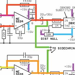
Keep RF suppression caps as close as possible to the opamp, bypass caps
as well (though not as critical as RF ones).
What's most important, however, is to be ready to redo a complete design twice or three
(ten) times over. This is the nastiest thing everybody keeps dancing around like a boiling
cauldron, because it's where the work is, but it's just where all the flavor is.
Anyway...
Here's my personal approach:
1. Look at your box layout. Where are the knobs and switches, where are your XLRs, IECs,
etc. and design PCBs to accomodate these with Lorlin footprints, pin headers, pcb-mount
XLRs (Try Neutrik B) and bypass relays. It just makes sense.
2. Get with the guts - keep the PSU and trafo away from unbal signal path stuff (although
you'll always see designs with Trafo immensely close to signal traces that are dead quiet)
and let your design flow around your interface boards. This way, you can also avoid el messo wiro.
In Practice, you'll always end up going back and forth between 1. and 2. (and using some
interesting language as you do).
3. Make individual boards for new ideas that connect directly side-by-side with pin
headers – that way, if you group everything together on one big board, you can just
drop the headers and connect the traces in 5 minutes, knowing it'll work.
4. Don't try too much at once. You'll go to the flippin' nuthouse if you do. Start small.
Think Forrest Gump: "Well, so I thought I'd run to the end of the property...and when
I got there, I thought maybe I could run to the city limit...and when I got there,
I thought I could run to the edge of the county...then the state...then suddenly...I
reached the ocean".
5. Design with serviceability in mind. Nothing pisses me off more than an ultra-confounded
design where everything is soldered to everything and you can't get the flip in there and take
it apart logically. Take a look at Neumann casettes, they rule. Think hinges, headers,
spacers, modules. It's a rough world, and your builds will fare better for being accessible
rather than being proprietary send-it-in bullshit that's impossible to fix yourself,
unless you have access to somebody with long hair, a goatee and a death metal t-shirt.
This really puts the fun back in fixing too because you can determine faulty board,
out mit za oldt boardt, undt - macht schnell - in mit za new. Dot's vot I zay. Ziss vey
you can remain operational betta fasta cheapa, ja? You can debug za defunct boardt
on down time, ven you are not preoccupied mit moar dairectly relevant
functions.
Also, if it's an original design and you're in running production, assembly is reduced to
k'nex logic.
6. Contemplate. Don't be surprised to find yourself
staring at your layout, not doing anything.
Your mind will be making connections, placing components and laying things
out while you just sit there and drool. This is serious work. You're not wasting time.
Be patient with yourself, and be kind with yourself when you don't get as far as you wanted.
7. Make a couple standard designs to get to know the material. Do some different PSUs,
some different bal I/O's, switching boards, the lot. Your brain will integrate this stuff
soon enough and suddenly you can do things from a higher perspective, like cooking.
If you understand the function blocks you'll understand the device.
8. Get a caliper, and use it. I prefer metal scale over digital scale because metal scale doesn't
break. Measure out footprints of the components you want to use that aren't in the standard
raster of 0.1 in. Get on youtube and get some instructions, the thing can do more than you'd
give it credit for. You can use it on just about everything.
9. Component placement is everything. It's like Sudoku or Tetris - if your placement
is intelligent and de-cramped, your traces will flow naturally. This is just a matter of practice
and experience, what was hell yesterday is "ah, yeah, before breakfast" tomorrow.
10. Simplify, Simplify. Get things optimized. How can you make things nice to assemble?
Can you get individual wire connectors put together in a single group header? Can you route
things so that headers are nice and side by side? Are there too many Opamps in the signal path
as a residue of previous designs that can be removed? Are function blocks distributed such that
you have to keep sending signals around the box 3 times before they get to their destination
when you could solve it in a way that it's straight, neat and short? Is there redundant stuff that
you just don't need? Reduce to what really matters. In the end, when you think through your
design in your mind, things should just go "aaaaaahhhhhh niiiiice". High tech, maybe, but common
sense for sure.
Remember - Designing great audio ≠ Designing great box.
Getting Illustrator to sit up straight and not play with its food
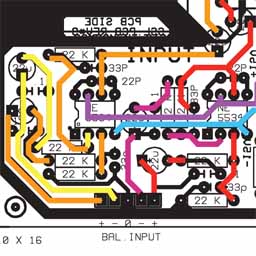
Make separate layers for pads, traces, components and text. This is essential. You won't believe
the work I get into when someone's designing something and then just "somehow" blindly
stitches it all together on a single layer or possibly two because he's a) lazy, b) in a hurry,
c) doesn't know better or d) is "above it all" because he's too busy "being inspired" to be
bothered with it – it's just nasty, and I have a chainsaw, a bathtub and some nice relaxing
H2SO4 for people who do that.
You can get a handle on layers by making them all first over in the layers palette and then
sorting them in the order of:
Top Components
Top Descriptions
Bottom Components
Bottom Descriptions
Pads (with holes)
Top SMD Pads
Top Text
Top Traces
Bottom SMD Pads
Bottom Text
Bottom Traces
Mount holes
Board Outline
Omit whatever you don't need, but don't change that order. Lock the Board Outline layer
with the little box next to the visibility box so that you don't keep selecting the board and
moving it around accidentally. The reason for separate SMD and through-hole pad layers
is because of side separation on one hand, but also because you can simply export the SMD
Pad layers as DXFs and boom - you have an SMD paste dispensing mask you can have
lasered (which you can already work with using a cheap metal spatula that has a sharp blade
and masking tape to stick it in position on the board once you get there. Costs little and
saves time, and your arm, dispensing the stuff by hand pressing a rock-hard plunger).
Do this once with success and you'll never look back, because it rocks house
that big.
Text on the top layer is legible, text on the bottom, backwards (right-click -> Transform
-> Reflect (axis vertical)). Always. When you do a layer separation for etching, reflect
the entire top layer, leave the bottom layer as it is, print and you're good to go. You can
get some pretty funky mirror action going on in your mind trying to understand how this
works, and better yet, you'll have forgotten again by tomorrow.
When you work in Illustrator, the last thing you had selected defines the properties of the
next thing you'll create - stroke width, fill and stroke colors, and what layer it ends up on.
You can utilize this all the time when you want to make new things, just select the object
you want to mimic on the layer you want to draw on and go from there. If you screw up
and design something on the wrong layer, just select it, then select the layer you want it
on, then right-click -> Arrange -> Send to current layer.
To make a pad, take the ellipse tool and click somewhere, then enter 1.4mm width and height.
Set fill color to white (colors palette) and stroke color to black, set stroke width to 2.2pt
(little box at the top, sometimes you have to click an object twice with the select tool, V).
You now have a pad. Now right-click -> Transform -> Move (Ctrl/Cmd-Shift-M) and type
in 0.1in or 2.54mm horizontal. Hit "copy". Now press Cmd/Ctrl-D 6 times. Now go back
to the move dialog. Enter 0 horizontal, 2.54mm*4 or 0.1in*4 into vertical and hit copy.
Now select all the pads and group (Ctrl/Cmd-G). You now have a DIL16 footprint.
Double-clicking it gives you isolation mode, so you can edit stuff in a group now without
having to resort to the infamous little white arrow that turns Illustrator into a shooting gallery
(direct select tool, A). It's a cool tool to use, you edit the points of something rather than
the thing itself. Name the Group "DIL16" in the layers palette (with the little triangle by
the layer's thumbnail to unfold objects, you'll see what's selected by the little circle on the
side. This circle is how to select stuff from the Layers Palette, btw). Do that once and all
the copies will have that name from there on out, so you'll know what's what in the layers
palette. If you bastardize it to DIL8 by going into iso and removing 8 legs, rename it.
</sermon>
Learn to construct everything geometrically -
numerically. Forget Snap To Grid, it doesn't work.
Try it and you'll see - groups have their own center. Move things in 0.1in (2.54mm) steps.
Work down to 1/1000th mm precision, it takes just as long as working to looser tolerance.
I do a whole ton of translations in Illustrator's move dialog, with the copy button. Use
groups, isolation mode, smart guides, and the shift key when working the pen tool. As
a general rule, the fewer anchor points a path has, the better. If you want two things to
line up then select one and copy its x or y location from the transform window. Then select
whatever's supposed to line up and paste that value into its box in transform, and that's it.
Here's the coolest thing on Earth: When you want boards to connect with each other vertically,
you can place a pinheader somewhere and then hit Move, set H and V to 0, 0 and hit copy.
Now select the pad layer for board number 2, then right-click - Arrange - Send to Current
Layer. Bam - Aligned. Kicks Ass.
You can design the whole front panel right on top of this, all in the same program - you never
have to worry that it won't line up because it's all right there. Ah, there's beauty.
One document and everything in it. :-*
Alt/Option-dragging with the V (select) tool copies stuff. Alt/Option dragging and pressing
the shift key once you're dragging copies stuff in a straight line. Shift-clicking stuff adds
objects to the selection or removes them from it.
Alt/Option-mousewheel is zoom on cursor. This is the only navigation tool you'll ever need.
If your mouse doesn't have a wheel, it sucks. It's either the navigator window or space for
the little drag hand and Z for Zoom tool.
More keystrokes are A, V, P (Aliens vs Predator) and Shift-C (which when in pen mode
is accessible momentarily by holding Alt/Option).
This is the tip of the century: If you have a mouse with a thumb button, configure it to do
the "Ctrl/Cmd-Z" (undo) keystroke. You will LOVE it. If you have more buttons, "redo" and
"Ctrl/Cmd-Shift-M" (move) are golden.
The Transform box within Illustrator accepts math input. So, if you need to move a resistor
one step to the left and it's at 215.365mm in x, type in 215.365-2.54 and you'll get it in
the right place. You can even do metric/imperial mishmash, telling it "35.32mm-0.2in".
Try not to go under 2pt stroke width for traces when interfacing with soldering pads. Doing
1pt traces is electronically sound very often, but when you get close to a pad that is gonna
see the soldering iron, this leads to entire afternoons of swearing and cursing and making
coffee.
When you want to make a trace longer, move the pen tool over an endpoint (anchor) of the
path until it gets a little slant next to it. Generally there's a little x, that means start new
path, the slant means continue a path, little plus adds points to a path and little minus
removes them again. Get the hang of the convert anchor tool - Shift-C. Click on a point
to steal its tangents/handles, and click and drag to put them there again - great if you're
doing symmetrical work. Use the shift key profusely. It'll keep things in line.
Setting up for printout is simple. Locate the artboard tool (shift-O) and set the artboard size
by dragging the corners of it. Then to set up the area that gets printed, well, that tool is hiding
behind the little hand tool at the very bottom of the tools palette. It's called the print tiling
tool, and it doesn't have a keystroke. You can paypal funds for coffee to thelema*att*lol.li.
Page setup is not where it should be in CS4. You have to hit Print, wait till it brings up the
dialog and then you can select it with a button. Grr. Adobe peeps didn't have anything
better to do.
Print out your layout on paper, put it on a piece of styrofoam, and stick your components
in there to check for clearances and pin spacing, making sure everything fits nicely.
When exporting dxf or the like for things like SMD masks and big machines in general,
convert everything to paths that isn't (like text) by selecting it and then right click -
Create Outlines. Next,
ungroup everything (i.e., hide all other layers, select all and
then button-smash Ctrl/Cmd-Shift-G) and export in the stupidest Autocad format there is.
You won't believe what you're in for when the guy who runs the laser is using something
like PEPS for DOS as a final control surface and your pads end up all over the place
while he explains to you with great detail and accuracy why modern software sucks.
He then goes on to brag about how he can shoot a .02 mm hole into a pre-milled
metal doodad at 1µm tolerance. Amazing guy. Built that laser himself.
Before you dunk anything into the acid, take your schemo and do a
check of
every single
node, crossing components out that are wired correctly. By this time you'll be itching at the
groin to get the darn thing built, but you'll probably inadvertently have made six very serious
mistakes that'll come back to forcefully and repeatedly insert things which satisfy the
dimensional criterion y ≥ 2x into places that require separate adaptation for this purpose
(which at least partially violates the limits of originally specified design constraints) but
exhibit surprising tensile tolerances when subjected to the correct and precautious
employment of commonplace or
naturally occuring mechanical aids of up to 5 times the
diameter stated in the absolute maximum ratings (or greater) should you choose to forego
this element of procedure without prior consideration of applicability pertaining to the law
of cause and effect and the manner by which it applies to the point of elaboration hereby
presented and elucidated. Don't say I didn't warn you. If you don't check your work, better
have lubricant. Being a dumb ape gets punished
without mercy. No offense to apes.
One thing I like about freehand designing is that it lets you do things simply that are otherwise
difficult (like custom board shapes and whatnot) and it forces your brain to think like the
schemo at all times. You will never be closer to your design than this - there's no computer
there to help you, and in a while you'll get to know the full power of your subconscious,
which suddenly makes designing a hell of a lot easier because you're so "in there". It really
pays off. Then, try to see if you can stick with single-layer designs using as few links as
possible. This way, you'll start with the hardest thing on earth and when you do get to
dual layer it'll be like cream cheescake, a warm bathtub and a glass of champagne (or
similar supplements congruent in nature). If for no other reason, because it's highly etchable.
That said, it's sometimes a great idea to do something in Eagle or so first so that you can
quickly determine good placement with the rubber band function before you go on.
And never let yourself be put off if it doesn't work to begin with. Generally, 90% will be working
just fine, but the remaining 10 enjoy giving you the feeling you just built a piece of crap. The
reasons for it at times will seem downright esoteric. There is no such thing as "esoteric". Either
it works, or it doesn't, and that's because it's built right, or it isn't. There is no such thing as
an issue you cannot ultimately understand. This is also where the real fun is, though, because
after hours with a pair of headphones, a probe, a pair of pliers, soldering iron, pen, schemo,
copy of the traces and resistors flying all over creation suddenly it goes *click* and you hear
fantastic working audio...
...and that's Heaven, right here on Earth, smiling at you going "see, it wasn't that hard after
all. You can do it."
And then you rack it, and then you
make music with it.
And this is when the real ideas begin to pour in.


") )
)